EN_US

PCB Design & Layout Service

With 22+ years of expertise, we ensure efficient prototyping, EMI/EMC mitigation, and production-ready layouts for diverse industries. UMEC delivers custom, high-speed, and RF PCB designs optimized for signal integrity, manufacturability, and performance.

PCB design services

Schematic Capture

This initial step leverages specialized software to accurately place and connect components, forming a robust blueprint for subsequent design phases. This ensures precise circuit design, clear documentation, and smooth collaboration throughout your PCB design process.

1. Schematic Capture

Schematic Diagram Design

Captured data is transformed into a clear visual diagram detailing component relationships and connections with standardized symbols and notation. This concise representation ensures design clarity among engineers and stakeholders, forming the foundation for efficient PCB development.

2. Schematic Diagram Design

PCB Layout

Once the schematic is finalized, this stage focuses on placing components on the physical board with optimal signal routing, minimal interference, and efficient space usage. The outcome is an optimized, high-quality design that prioritizes signal integrity, reliability, and cost-effective manufacturability.

3. PCB Layout

Simulation Testing

Before physical production, simulation testing models the PCB’s electrical behavior under various conditions, validating circuit functionality, identifying potential issues, and optimizing performance. By reducing design risks and enhancing reliability, this phase upholds KINGBROTHER’s high standards while ensuring compliance and robust performance.

4. Simulation Testing

EMC/EMI Analysis

Electromagnetic Compatibility (EMC) and Electromagnetic Interference (EMI) analysis ensure the PCB complies with regulatory standards. This analysis identifies potential interference sources and applies design techniques to minimize emissions and susceptibility.

UMEC incorporates these practices to ensure that its products operate reliably in diverse electromagnetic environments.
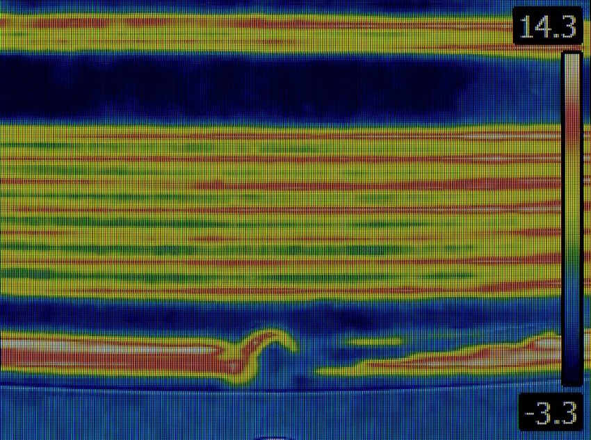
5. EMCEMI Analysis

Thermal Analysis

Thermal Analysis evaluates how heat is generated and dissipated across the PCB, pinpointing hotspots and guiding component placement, cooling mechanisms, and material choices. Incorporating thermal management strategies ensures consistent performance, prolongs component life, and maintains reliability under high-power conditions.

6. Thermal Analysis

Design Modification Service

Recognizing that iterative improvement is often necessary, this service allows for quick modifications based on feedback or evolving requirements. Changes can include component swaps, layout adjustments, or enhanced features to meet emerging market demands.

UMEC’s proactive design modification process enhances product longevity and adaptability.

7. Design Modification Service

Design for Manufacturability (DFM)

DFM tailors the PCB layout to streamline and optimize the production process by focusing on component spacing, trace widths, and overall board structure. UMEC’s approach reduces costs, minimizes errors, and maintains exceptional quality—ensuring reliable, high-volume manufacturing.

8. Design for Manufacturability (DFM)

Characteristics & Advantages

Using flexible PCB design guidelines and industry best practices to ensure your PCB meets manufacturability and reliability requirements. We offer:

Custom PCB Design

Tailored to meet unique applications — be it consumer electronics, industrial automation, medical devices, aerospace, or military-grade systems.

Signal integrity & power integrity analysis

Including thermal simulation and EMI/EMC mitigation strategies

Design for Manufacturing (DFM) & Design for Test (DFT)

Including automated Gerber checks and panelization.

KB EDA Design Software

KBEDA is a secondary development tool for Cadence Allegro, offering over 400 functions with copyrights and patents. It improves design quality and shortens development cycles.

Typical PCB Design Process

From concept to prototype, UMEC provides comprehensive PCB design services to accelerate your product development.

Our expert team ensures high performance, cost efficiency, and seamless manufacturability.

Requirement Gathering

We begin by identifying and documenting project goals, customer needs, and technical specifications to determine essential features, performance criteria, and constraints. This thorough approach ensures a clear roadmap that captures all crucial requirements for a successful outcome.

Schematic Design

Develop detailed circuit diagrams to capture the functional design, selecting suitable components and establishing robust electrical connections to ensure overall feasibility.

PCB Layout

Translate the schematic into a physical board layout, optimizing component placement and routing for signal integrity and manufacturability while adhering to design guidelines.

Testing and Revision

Conduct comprehensive testing on prototypes to evaluate functionality, reliability, and performance. We then gather test data, identify issues, and refine the design iteratively until all desired criteria are met.

Prototype Manufacturing

We produce initial prototype boards based on the validated PCB layout, collaborating closely with our manufacturing partners to ensure each prototype meets stringent quality standards.

Simulation and Validation

We run electrical, thermal, and signal integrity simulations to verify the design’s performance under diverse conditions, then fine-tune the design to meet all required specifications.

Output Documents From Our PCB Design Services

Gerber Files

Contains all the manufacturing information for each layer of the PCB.

Bill of Materials (BOM)

A detailed inventory of components, complete with part numbers and specifications.

Schematic Diagram

A clear representation of the electrical connections between components.

PCB Layout Files (Stack-up)

Files showing the physical layout of the components and traces on the PCB.

Assembly Drawing

Instructions for assembling the components on the PCB.

Pick and Place Files

Essential data for SMT assembly and assembly work.

D Model PDF

A visual representation of the board for better understanding and analysis.

Test Plan (optional)

Details on testing procedures to ensure the PCB works as expected.

Other customer-specified outputs

Get expert advice on your PCB design